NanoBat at MRW – MIKON 2022
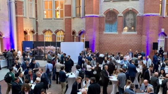
This year‘s MIKON conference, a bi-annual international event as part of the Microwave and Radar Week (MRW), took place in the beautiful city of Gdansk, Poland on the campus of Gdansk University of Technology. NanoBat partner QWED has been involved with MIKON for several decades (see the report about MIKON 2020 and the article on Women in Microwave published in IEEE Microwave Magazine. This close connection gave the NanoBat project the great opportunity to be present with various activities:
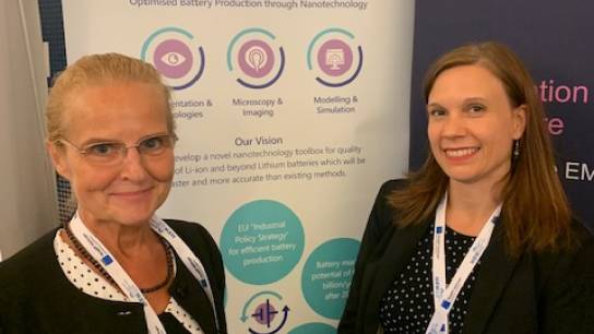
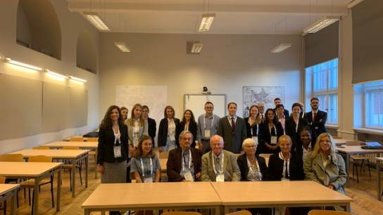
1. Women in Engineering Matinee (as part of IEEE WiE activities) on Monday, 12.09.2022 Technical session followed by panel discussion on any topics of common interests. The Matinee was organised by QWED and sponsored by NanoBat. It featured a number of talks providing a perspective of women working in research & science. NanoBat contributed to this workshop with a talk from Janine Jost (EURICE) about “Women in EC funded Projects – Challenges & Opportunities” using the NanoBat project as a case study. More information on the programme and speakers is available here.
2. Short Course on EM Modelling
(co-organised with EM Invent) on Thursday, 15.09.2022, morning
Intro lectures, case-studies, hands-on experience with QuickWave (FDTD) and InventSim (FEM)
3. Workshop on Materials' Characterisation in Microwave and Millimetre-Wave Range
(co-organised with EMARGES) on Thursday, 15.09.2022, afternoon
Intro lectures, case-studies, hands-on experience with GHz resonators operating with VNAs and Q-Meters
In addition to these workshops and courses, NanoBat had also four papers published and presented during MIKON conference:
1. Open Platform Tools to Modelling Electrochemical Phenomena in Solid Electrolyte Interphase
Authors (presenter first): Lukasz Nowicki; Malgorzata Celuch; Marzena Olszewska-Placha and Janusz Rudnicki (all QWED)
Abstract: The paper reports recent developments of numerical methods in the framework of the EU H2020 NanoBat project. It presents an extension of the computational electromagnetics platform, previously extended to electrochemistry, to the modeling of coupled electrochemical phenomena occurring at the solid electrolyte interphase. Two new FDTD algorithms have been developed to solve coupled Poisson and drift-diffusion equations and electric double layer using FDTD method. All developments are prepared for use in modeling of industrially representative test fixtures for battery materials, under the open license of the H2020 NanoBat project.
2. Contactless Device for 2D Imaging and Precise Characterisation of Electrical Parameters of Anode Materials for Battery Cells
Authors (presenter first): Marzena Olszewska-Placha (QWED); Athanasios Masouras (PLEIONE); Andrzej Wieckowski (QWED); Ntorella Chotza (PLEIONE); Malgorzata Celuch (QWED) Abstract: This work is dedicated to developing new test-fixture for precise characterisation and both, quantitative and qualitative 2D imaging of thin conductive layers used for anodes in battery cells. The device is based on Single-Post Dielectric Resonator method, serving as a microwave probe, adopted to be used in a 2D scanner configuration. The device is designed with the aid of rigorous electromagnetic modelling, taking advantage of its axial symmetry, which is further used for development of a dedicated measurement software transferring resonant frequency and Q-factor of an empty and sample-loaded device into electrical parameters of a sample under test. The designed test-fixture is validated on reference materials samples and further applied to battery anodes material layers for their parameters uniformity evaluation and quality testing.
3. 2D Imaging Technique for Quantitative and Qualitative Characterisation of High-Resistivity GaN Semiconductor Wafers for Light and Power Electronics
Authors (presenter first): Marzena Olszewska-Placha (QWED); Ewelina Mozdzynska (Lukasiewicz Research Network -IMiP); Janusz Rudnicki (QWED); Malgorzata Celuch (QWED)
Abstract: In this work an automatic SPDR scanner is applied to 2D surface imaging of electrical parameters of GaN semiconductor wafer. The homogeneity of electrical parameters of GaN template is crucial for light and power electronics allowing for enhancing packaging efficiency and obtaining high quality and repeatability of resulting devices. For the first time, the new 10GHz SPDR scanner is applied to obtain 2D resistivity map of GaN template delivering both, quantitative and qualitative measure of inhomogeneities of the semiconductor structure.
4. GHz Characterisation of Dielectric Properties of Ultra-Low Temperature Co-Fired Ceramic Materials for 5G Systems Application
Authors (presenter first): Marzena Olszewska-Placha (QWED); Dorota Szwagierczak and Beata Synkiewicz-Musialska (Lukasiewicz-Institute of Microelectronics and Photonics); Janusz Rudnicki (QWED); Jan Kulawik (Lukasiewicz-Institute of Microelectronics and Photonics, Poland)
Abstract: This work is dedicated to non-destructive characterization of dielectric properties of novel ultra-low temperature co-fired ceramic materials. With regards to their targeted application to emerging 5G communication systems, high accuracy measurements of complex permittivity are of crucial importance for materials manufacturers and further, 5G components designers. For high system efficiency, the discussed materials are aimed at low dielectric constant, in the range of 4-6.5 and low loss tangent, being within the range of 0.0005-0.005. Complex permittivity extraction is performed with the aid of split-post dielectric resonator method, which has been known for its robustness and high accuracy.
More information on the conference and the venue can be found on the conference website.
For more details and pictures about our NanoBat activities, visit QWED’s website.
